
DongGuan Tuopst Technology Co.,Ltd
One-Stop Manufacturer for PCB/PCBA, Plastic parts, Metal parts
Tuopst@126.com ,+86 13580576967
One-Stop Manufacturer for PCB/PCBA, Plastic parts, Metal parts

Advanced Multilayer PCB Manufacturing
Equipped with cutting-edge technology to ensure the stability and reliability of high-layer PCBs.

Fast Delivery
Streamlined production processes to shorten lead times for multilayer PCBs

Flexible Customization
Offering diverse customization options for multilayer PCBs to meet various application needs.

Strict Quality Control
Every production stage is rigorously inspected to ensure multilayer PCBs meet international standards.
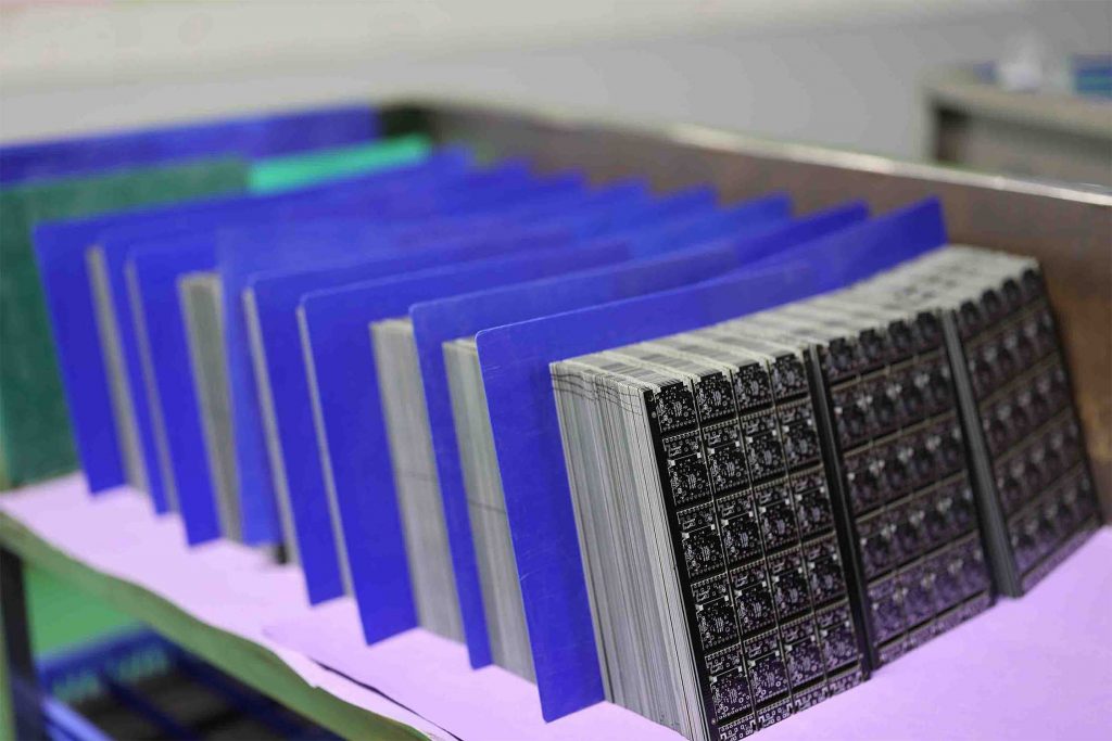
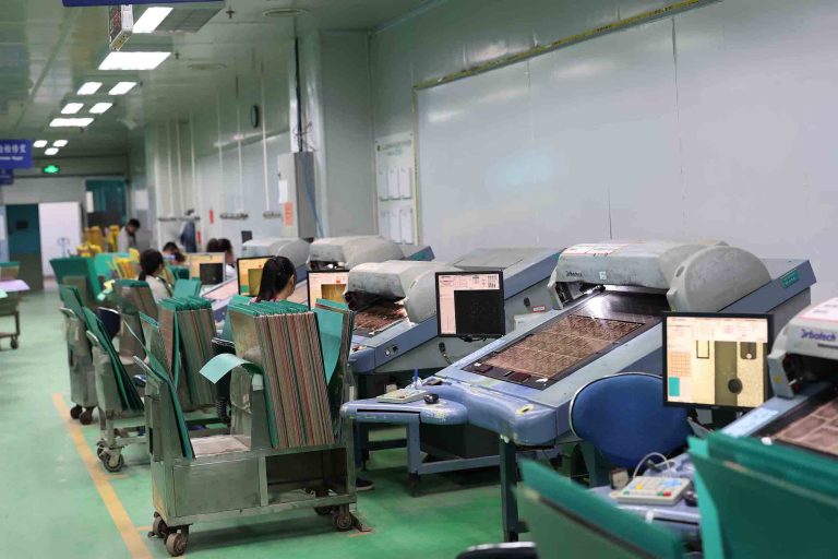
Our factory specializes in the production of high-quality multilayer PCBs, utilizing state-of-the-art equipment and technology. We are capable of producing multilayer PCBs with a high layer count, ensuring stability, reliability, and optimal electrical pe
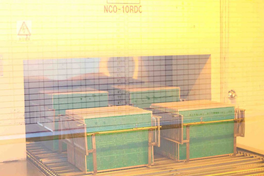
With a well-organized production system and efficient workflow, we minimize lead times for multilayer PCB manufacturing. Our experienced team and optimized supply chain allow us to quickly turn around even large and complex orders without compromising on
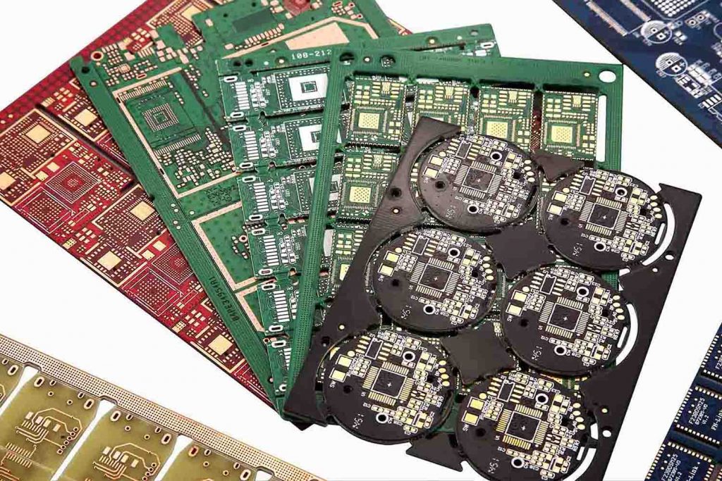
We understand that different industries and projects have unique requirements, which is why we offer a wide range of customization options for multilayer PCBs. From material selection to layer count, thickness, and layout design, we collaborate closely wi
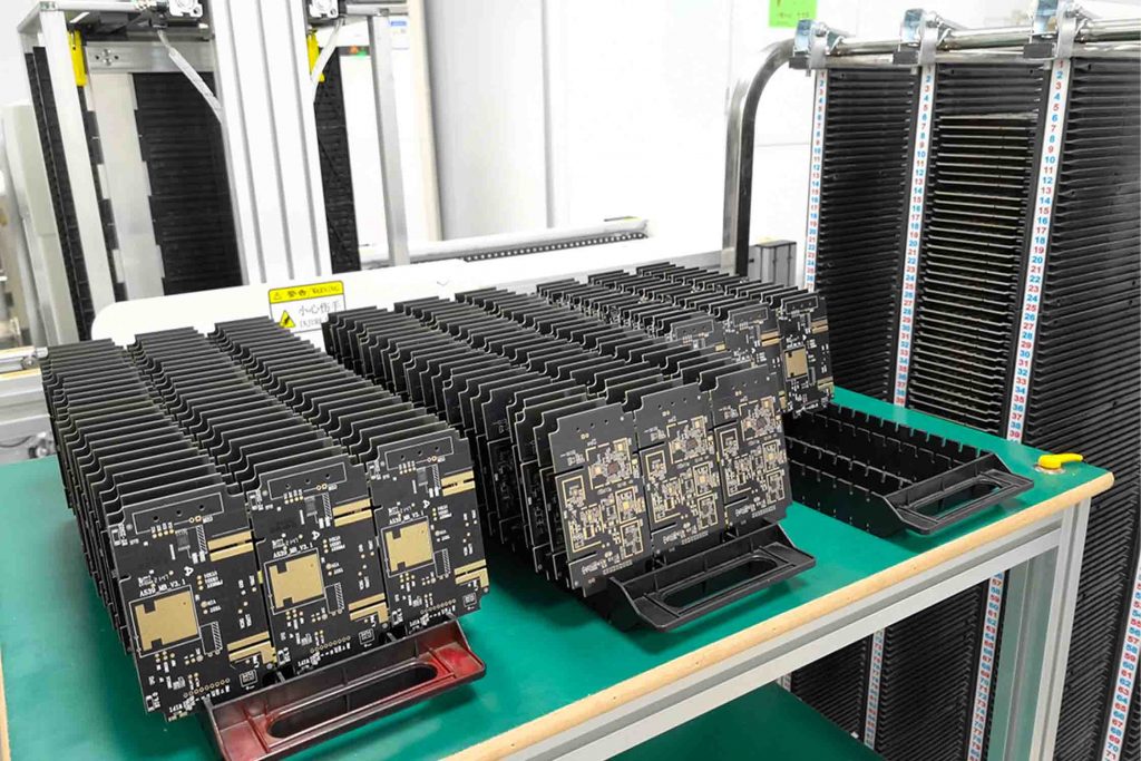
Quality is our top priority, and we implement rigorous testing and inspection procedures throughout every stage of the multilayer PCB production process. From raw material inspection to in-process quality checks and final testing, we ensure that each PCB
Items |
Multilayer PCB |
Material |
Lead-free、Halogen-free、H-Tg、Low loss |
Layers |
1-40L |
Max cut lamination size |
Min3*3mm-Max1200mm |
Final board thickness |
0.18-5.0mm |
Min Final Hole size |
0.075mm |
Aspect Ratio |
14:1 |
Inner layer Line Width/Space |
0.05mm |
Copper Foil Thickness (Inner Layers) |
1/2oz~3.0oz |
Min dielectric layer thickness |
50um |
Copper Foil Thickness (Outer Layers) |
Hoz-14oz |
Copper to drill distance |
0.2mm |
Out layer Line width/space |
0.05mm |
Min SMD width |
0.05mm |
Max Solder Mask Plug Hole Diameter |
0.5mm |
Solder mask strip width |
0.075mm(Green/1OZ) |
Final Set Size Tolerance |
±0.1mm/limit±0.05mm |
Min Hole to board edge Distance |
0.15mm |
Min Beveling angle Tolerance |
±3-5° |
Layer to layer Tolerance |
≤0.075mm(1-6L) |
Inner layer Min PTH Annular Ring |
0.15mm |
Out layer Min PTH Annular ring |
0.15mm |
Surface Treatment |
OSP、HASL 、ENIG、Gold Finger、Plating Gold 、ENEPIG、IMM TIN、IMM AG |
Warp&Twist |
≤0.5% |

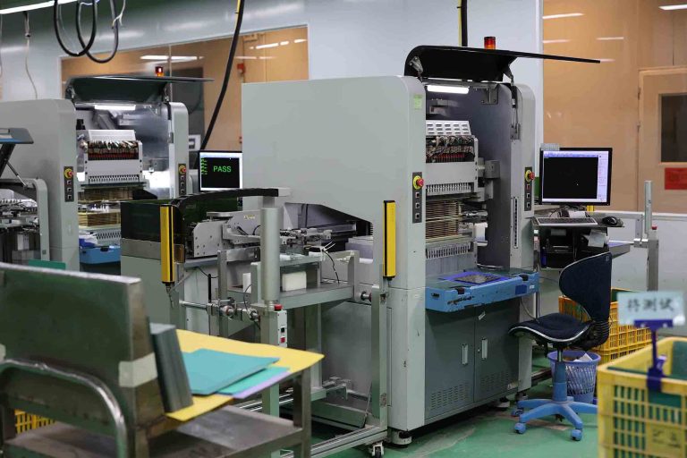
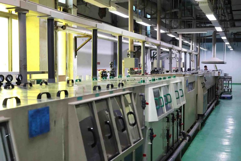
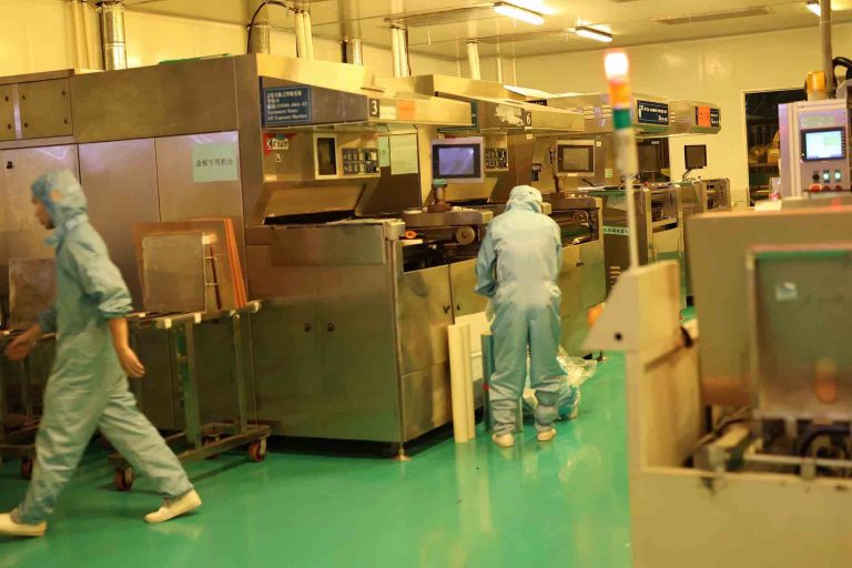
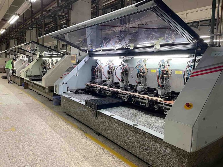
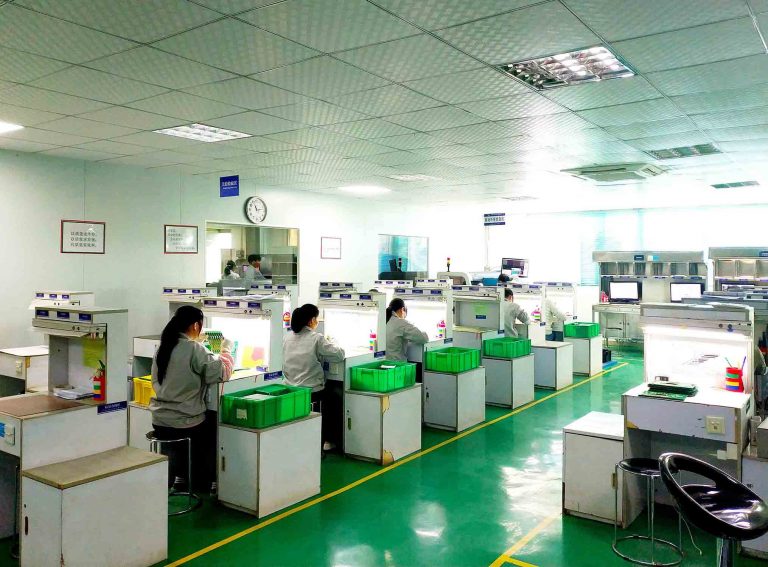
We can offer up to 24 to 40-layer boards with the highest degree of precision.